
The photonic path to quantum advantage

Quantum technologies are moving towards practical solutions in computing, sensing and secure communications, with photonics driving scalability and connectivity.
It has been an eventful year for quantum science and technology. Celebrated as the International Year of Quantum Science and Technology (IYQ) 2025, the year culminated in a Nobel Prize in Physics for pioneering work that laid the foundation for superconducting quantum technologies. Moreover, a steady stream of announcements has brought quantum information technologies closer to real-world applications and a global quantum race is underway, with nations, economic blocs and major tech companies viewing these technologies as critical to future geoeconomic competition.
Various technologies are competing in demonstrating practical quantum applications. Whether it is superconducting circuits, trapped ions, spin circuits or neutral atoms, photonics is expected to play a vital role in advancing quantum technologies, especially in the transfer of information in interconnected and distributed quantum computing architectures. In this issue of Nature Materials, we present a Focus that explores the role of photonics in advancing quantum information technologies.
In a Review, Hui Wang and colleagues discuss advances in quantum light sources, circuits and single-photon detectors that have accelerated progress across various applications; fibre-based quantum communication is already enabling short-range commercial applications, while satellite-based quantum key distribution offers a preview of future global networks. In quantum computing, reducing photon loss is crucial to building error-corrected systems and implementing loss-tolerant encoding for both computation and quantum repeaters, and in quantum metrology, the use of entangled photons may lead to surpassing classical precision limits in gravitational-wave detection, optical clocks and biological imaging. Looking towards commercialization, integrated photonics and hybrid systems offer a pathway to scalability, while challenges such as decoherence and detector inefficiencies are being addressed through improved materials and error-correction techniques.
Integrated photonic technologies provide such scalability and are gaining attention and investment as a key solution for high-speed, energy-efficient data transfer in artificial intelligence and data centre infrastructures. Thus, their maturity also makes them well suited for commercializing quantum technologies. In integrated quantum photonics, platforms such as silicon-on-insulator, silicon nitride, indium phosphide, lithium niobate, gallium arsenide and silicon carbide (SiC) are being studied, and hybrid integration combining the features of some of these materials offers opportunities for improved generation, manipulation and detection of quantum states of light.
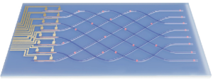
In an Article, Xudong Wang and colleagues report the building of hybrid quantum photonic chips using a precise transfer-printing technique to combine quantum dots with gallium arsenide waveguides and lithium niobate photonic circuits. The piezoelectric properties of thin-film lithium niobate allow strain tuning of each quantum dot locally, enabling dynamic control of their emission. Using this method, a hybrid chip with more than 20 single-photon sources is demonstrated (pictured). Crucially, by applying local strain, the team achieves high-visibility quantum interference between spatially separated single-photon sources. In a related News & Views article, Anna Ovvyan and Wolfram Pernice highlight how leveraging the electro-optic properties of lithium niobate can lead to fully controllable multi-functional quantum circuits for advanced optical computing on-chip.
When scaling qubit devices, noise poses a challenge because it limits how long quantum information can be stored, reducing the time available to perform multiple operations before errors occur. In an Article, Lucas Stehouwer and colleagues explore the use of epitaxial, strained germanium quantum wells in Ge/SiGe heterostructures grown on Ge wafers to demonstrate a considerable reduction in charge noise by suppressing disorder. Their systematic charge and magnetic noise characterization in complex spin qubit devices, integrating up to ten quantum dots and four sensors in two dimensions, highlights the need for full isotopic purification to enhance qubit coherence in scalable quantum processors.
Beyond computation, photonics can also enable quantum sensing solutions. In an Article, Pei Li and colleagues explore the quantum sensing capabilities of SiC, a material that combines broadband optical transparency and strong nonlinear optical properties and can host quantum sensors based on colour centre spin defects. Using room-temperature divacancy spin qubits in alkene-terminated SiC, quantum sensing for biological environments is proposed. These qubits operate at near-infrared wavelengths, minimizing interference with organic molecules and water, and support multiple sensing protocols for applications in bioimaging, radical detection and nanoscale nuclear spin sensing.
Finally, in a Q&A, Pascale Senellart-Mardon discusses the vantage point of photonics to develop distributed quantum computing architectures, the intriguing prospects of merging quantum computing with artificial intelligence and the challenges that the quantum race is posing to international collaborations.
While some scepticism persists within the research community and important engineering challenges warrant caution, quantum technologies are rapidly advancing towards practical applications, with photonics offering a pathway to greater integration, scalability and efficiency.
link


